https://github.com/bennymeg/Fabrication-Toolkit
An JLC PCB Fabrication Plugin for KiCad
https://github.com/bennymeg/Fabrication-Toolkit
eda fabrication jlc jlcpcb kicad lcsc pcb pcba plugin toolkit
Last synced: about 1 year ago
JSON representation
An JLC PCB Fabrication Plugin for KiCad
- Host: GitHub
- URL: https://github.com/bennymeg/Fabrication-Toolkit
- Owner: bennymeg
- License: apache-2.0
- Created: 2022-06-02T16:40:46.000Z (about 4 years ago)
- Default Branch: master
- Last Pushed: 2024-10-14T19:30:37.000Z (over 1 year ago)
- Last Synced: 2024-10-21T03:45:45.572Z (over 1 year ago)
- Topics: eda, fabrication, jlc, jlcpcb, kicad, lcsc, pcb, pcba, plugin, toolkit
- Language: Python
- Homepage:
- Size: 1.14 MB
- Stars: 317
- Watchers: 11
- Forks: 53
- Open Issues: 7
-
Metadata Files:
- Readme: README.md
- Funding: .github/FUNDING.yml
- License: LICENSE
Awesome Lists containing this project
README

| **JLC PCB Plug-in for KiCad** |
|:-----:|
[](https://github.com/sponsors/bennymeg)
## Features
1. Generates gerber files in correct format for production
2. Generates BOM file in correct format for production
3. Generates Pick and Place file in correct format for assembly
4. Generates IPC netlist file
## Installation
### Official Installation
Fabrication Toolkit is distributed with the official releases of KiCad 6+. Open the "Plugin and Content Manager" from the KiCad main menu and install the "Fabrication Toolkit" plugin from the selection list.

### Manual installation
Download the [latest release](https://github.com/bennymeg/JLC-Plugin-for-KiCad/releases) ZIP file. Open the "Plugin and Content Manager" from the KiCads main window and install the ZIP file via "Install from File".
## Usage
Click on the Fabrication Toolkit  button on the top tool box inside KiCad pcb editor (pcbnew).
**⊛** Ensure your board is synchronized before invoking this addon [**F8**].
**⊛** The `User_1` layer in internally defined as a **V-Cuts** layer, please avoid using it for anything else (unless disabled). _(since v3.0.0)_.
## Options
Options can be set in the dialog that appears when the plugin is invoked. They are saved in a file called `fabrication-toolkit-options.json` in the project directory so that they are remembered between invocations of the plugin.

☑ __Archive name__: Name of the archive file to be generated. Can include text variables, such as e.g. `${TITLE}_${REVISION}`
☑ __Additional layers__: Comma-separated list of additional layers to include in the gerber archive.
☑ __Plot all active layers__: Whether to include all layers, instead of just the layers required by JLCPCB.
☑ __Set User.1 as V-Cut layer__: Merge User.1 layer with the Edge-Cut layer in production.
☑ __Use User.2 for an alternative Edge-Cut layer__: Use the User.2 instead of the Edge-Cut layer for the board outline in production. This is useful if you need process edges or panelization during production but still want to keep the individual outline for prototyping, 3D model exports, or similar purposes.
☑ __Apply automatic translations__: Apply known translation fixes for common components.
☑ __Apply automatic fill for all zones__: Refill all zones before generation production files.
☑ __Exclude DNP components from BOM__: Exclude components the had been set a DNP from th BOM.
### ① Include Component Part Number in Production Files
Add an 'LCSC Part #'* field with the LCSC component part number to the symbol's fields property.

#### Primary Fields*:
| 'LCSC Part #' | 'LCSC Part' | 'LCSC PN' | 'LCSC P/N' | 'LCSC Part No.' | 'JLCPCB Part #' | 'JLCPCB Part' | 'JLCPCB PN' | 'JLCPCB P/N' | 'JLCPCB Part No.' |
| --- | --- | --- | --- | --- | --- | --- | --- | --- | --- |
_The fields will be query in the order denoted above._
#### Fallback Fields*:
| 'LCSC' | 'JLC' | 'MPN' | 'Mpn' | 'mpn' |
| --- | --- | --- | --- | --- |
_The fields will be query in the order denoted above._
---
### ② Ignore Footprint in Production Files
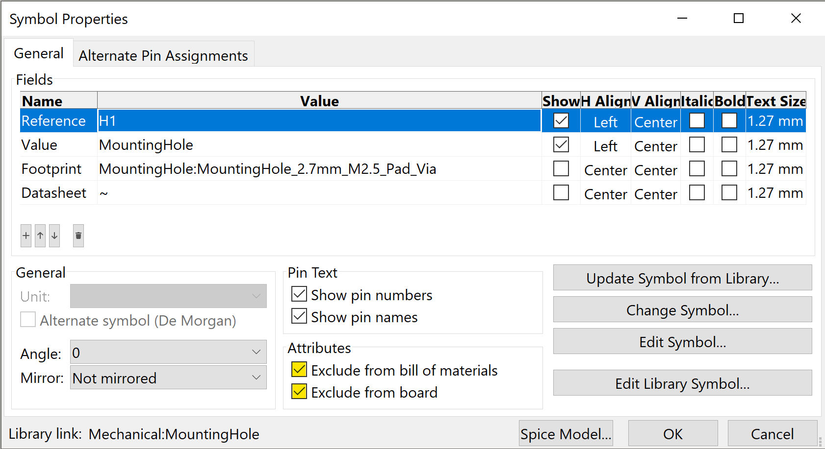
Select 'Exclude from board' or 'Exclude from BOM' in the symbol's attributes property in order to ignore the footprint from the relevant file.
Select 'Exclude from position files' or 'Exclude from BOM' in the footprint's fabrication attributes property in order to ignore the footprint from the relevant file.

---
### ③ Offset Component Rotation
The rotation of components in KiCad Footprints does not always match the orientation in the JLC library because KiCad and JLC PCB used different variation of the same standard. Most of the rotations may be corrected by the `rotations.cf` definitions. To the exception cases: add an 'FT Rotation Offset'* field - with positive values indicating counter-clockwise orientation offset in degrees.

If the JLC preview shows a footprint like this, enter a rotation offset of -90 to rotate pin 1 to the lower right corner.

As the rotation offset is entered in the Schematic Editor, make sure to update your PCB with the changes made to the schematic before generating a new set of production files, otherwise your changes won't be reflected.
#### Primary Fields*:
| 'FT Rotation Offset' |
| --- |
_The fields will be queried in the order denoted above._
#### Fallback Fields*:
| 'Rotation Offset' | 'RotOffset' |
| --- | --- |
_The fields will be queried in the order denoted above._
---
### ④ Offset Component Position
The position of components in KiCad Footprints does not always match the orientation in the JLC library because KiCad and JLCPCB used different variation of the same standard. To the exception cases: add an 'FT Position Offset'* field with an comma separated x,y position offset to correct it.
Use following table to quickly find out to which coordinate enter the correction based on JLC arrows clicks - depending on footprint rotation in KiCad PCB Editor status bar:
|KiCad footprint deg | x | y|
|----|----|----|
|0 deg, Front | right arrow | up arrow |
|0 deg, Back | left arrow | down arrow |
|180 deg, Front | left arrow | down arrow |
|180 deg, Back | right arrow | up arrow |
|90 deg, Front or Back | up arrow | left arrow |
|-90 deg, Front or Back | down arrow | right arrow |
For custom angles it's best to place also a temporary straight symbol to perform alignment.
Single arrow press in JLC is 0.0635mm (= 1/400in) shift.

As the position offset is entered in the Schematic Editor, make sure to update your PCB with the changes made to the schematic before generating a new set of production files, otherwise your changes won't be reflected.
#### Primary Fields*:
| 'FT Position Offset' |
| --- |
_The fields will be queried in the order denoted above._
#### Fallback Fields*:
| 'Position Offset' | 'PosOffset' |
| --- | --- |
_The fields will be queried in the order denoted above._
### ⑤ Override Component Origin
The Fabrication Toolkit reports the position of each component based on an automatically selected point of reference. This default behavior can be overridden by adding an 'FT Origin'* field to the component.
#### Primary Fields*:
| 'FT Origin' |
| --- |
_The fields will be queried in the order denoted above._
#### Fallback Fields*:
| 'Origin' |
| --- |
The **Origin** field supports the following values:
- `Anchor` - Uses the footprint's anchor point, which can be modified in KiCad's footprint editor.
- `Center` - Uses the center of the bounding box formed by the footprint's pads.
### ⑥ Override Component Layer
Some footprints may have their components defined on the opposite layer to there actual footprints. In these instances you can override mount side by adding an 'FT Layer Override'* field to the component.
The **Layer Override** field supports the following values:
- `top`, `t` - Override footprint layer to the top.
- `bottom`, `b` - Override footprint layer to the bottom.
#### Primary Fields*:
| 'FT Layer Override' |
| --- |
_The fields will be queried in the order denoted above._
#### Fallback Fields*:
| 'Layer Override' | 'LayerOverride' |
| --- | --- |
_The fields will be queried in the order denoted above._
## CLI
The plugin can also be used via the linux command line. This can be particularly useful if you need to embed the plugin into an automation pipeline or environment.
The plugin can be called with the command below:
```
python3 -m plugins.cli -p /myProject/myBoard.kicad_pcb
```
All the options from the GUI are also available via the cli interface:
```
python3 -m plugins.cli -h
usage: Fabrication Toolkit [-h] --path PATH [--additionalLayers LAYERS] [--user1VCut] [--user2AltVCut]
[--autoTranslate] [--autoFill] [--excludeDNP] [--allActiveLayers] [--archiveName NAME]
[--openBrowser]
Generates JLCPCB production files from a KiCAD board file
options:
-h, --help show this help message and exit
--path PATH, -p PATH Path to KiCAD board file
--additionalLayers LAYERS, -aL LAYERS
Additional layers(comma-separated)
--user1VCut, -u1 Set User.1 as V-Cut layer
--user2AltVCut, -u2 Use User.2 for alternative Edge-Cut layer
--autoTranslate, -t Apply automatic position/rotation translations
--autoFill, -f Apply automatic fill for all zones
--excludeDNP, -e Exclude DNP components from BOM
--allActiveLayers, -aaL
Export all active layers instead of only commonly used ones
--archiveName NAME, -aN NAME
Name of the generated archives
--openBrowser, -b Open web browser with directory file overview after generation
```
## Author
Benny Megidish