https://github.com/stffrdhrn/sdram-controller
Verilog SDRAM memory controller
https://github.com/stffrdhrn/sdram-controller
Last synced: 3 months ago
JSON representation
Verilog SDRAM memory controller
- Host: GitHub
- URL: https://github.com/stffrdhrn/sdram-controller
- Owner: stffrdhrn
- Created: 2015-05-07T22:11:10.000Z (about 10 years ago)
- Default Branch: master
- Last Pushed: 2017-05-13T10:05:08.000Z (about 8 years ago)
- Last Synced: 2024-11-10T00:32:56.046Z (8 months ago)
- Language: Verilog
- Size: 760 KB
- Stars: 306
- Watchers: 21
- Forks: 93
- Open Issues: 1
-
Metadata Files:
- Readme: readme.md
Awesome Lists containing this project
README
# _SDRAM Memory Controller_
`CURRENT STATUS : stable`
This is a very a simple sdram controller which works on the De0 Nano. The project
also contains a simple push button interface for testing on the dev board.
Basic features
- Operates at 100Mhz, CAS 3, 32MB, 16-bit data
- On reset will go into `INIT` sequnce
- After `INIT` the controller sits in `IDLE` waiting for `REFRESH`, `READ` or `WRITE`
- `REFRESH` operations are spaced evenly 8192 times every 32ms
- `READ` is always single read with auto precharge
- `WRITE` is always single write with auto precharge
```
Host Interface SDRAM Interface
/-----------------------------\
| sdram_controller |
==> wr_addr addr ==>
==> wr_data bank_addr ==>
--> wr_enable data <=>
| clock_enable -->
==> rd_addr cs_n -->
--> rd_enable ras_n -->
<== rd_data cas_n -->
<-- rd_ready we_n -->
<-- busy data_mask_low -->
| data_mask_high -->
--> rst_n |
--> clk |
\-----------------------------/
```
From the above diagram most signals should be pretty much self explainatory. Here are some important points for now. It will be expanded on later.
- `wr_addr` and `rd_addr` are equivelant to the concatenation of `{bank, row, column}`
- `rd_enable` should be set to high once an address is presented on the `addr` bus and we wish to read data.
- `wr_enable` should be set to high once `addr` and `data` is presented on the bus
- `busy` will go high when the read or write command is acknowledged. `busy` will go low when the write or read operation is complete.
- `rd_ready` will go high when data `rd_data` is available on the `data` bus.
- **NOTE** For single reads and writes `wr_enable` and `rd_enable` should be set low once `busy` is observed. This will protect from the controller thinking another request is needed if left higher any longer.
## Build
The recommended way to build is to use `fusesoc`. The build steps are then:
```
# Build the project with quartus
fusesoc build dram_controller
# Program the project to de0 nano
fusesoc pgm dram_controller
# Build with icarus verilog and test
fusesoc sim dram_controller --vcd
gtkwave $fusebuild/dram_controller/sim-icarus/testlog.vcd
# Run other test cases
fusesoc sim --testbench fifo_tb dram_controller --vcd
fusesoc sim --testbench double_click_tb dram_controller --vcd
```
## Timings
# Initialization
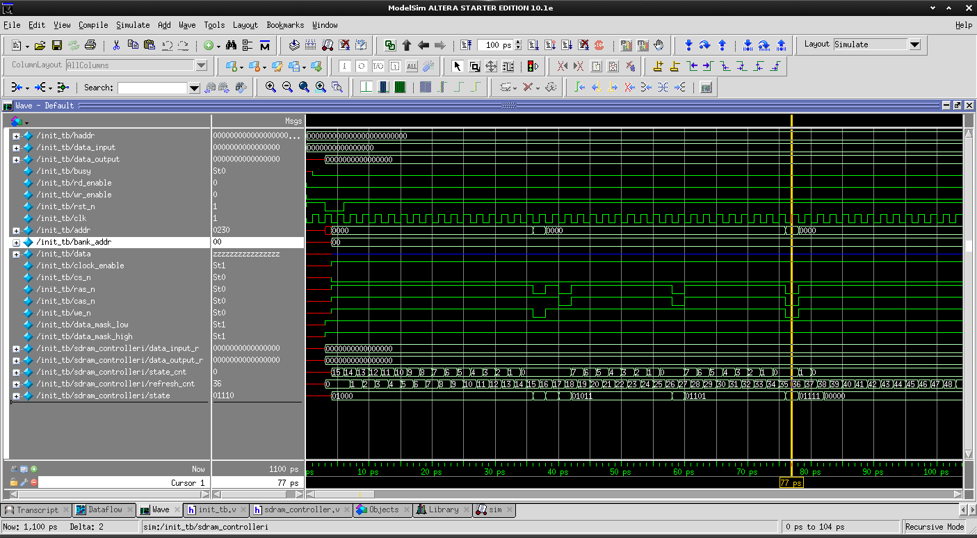
Initialization process showing:
- Precharge all banks
- 2 refresh cycles
- Mode programming
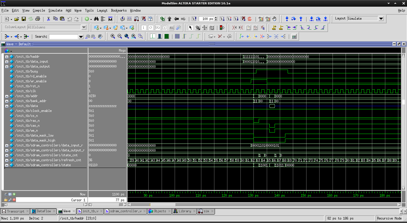
# Refresh
Refresh process showing:
- Precharge all banks
- Single Refresh
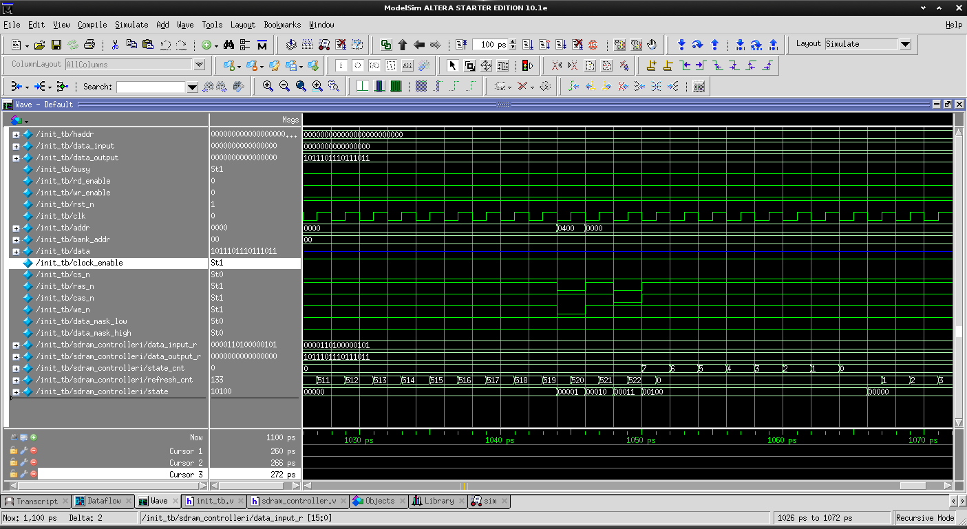
# Writes
Write operation showing:
- Bank Activation & Row Address Strobe
- Column Address Strobe with Auto Precharge set and Data on bus
# Reads
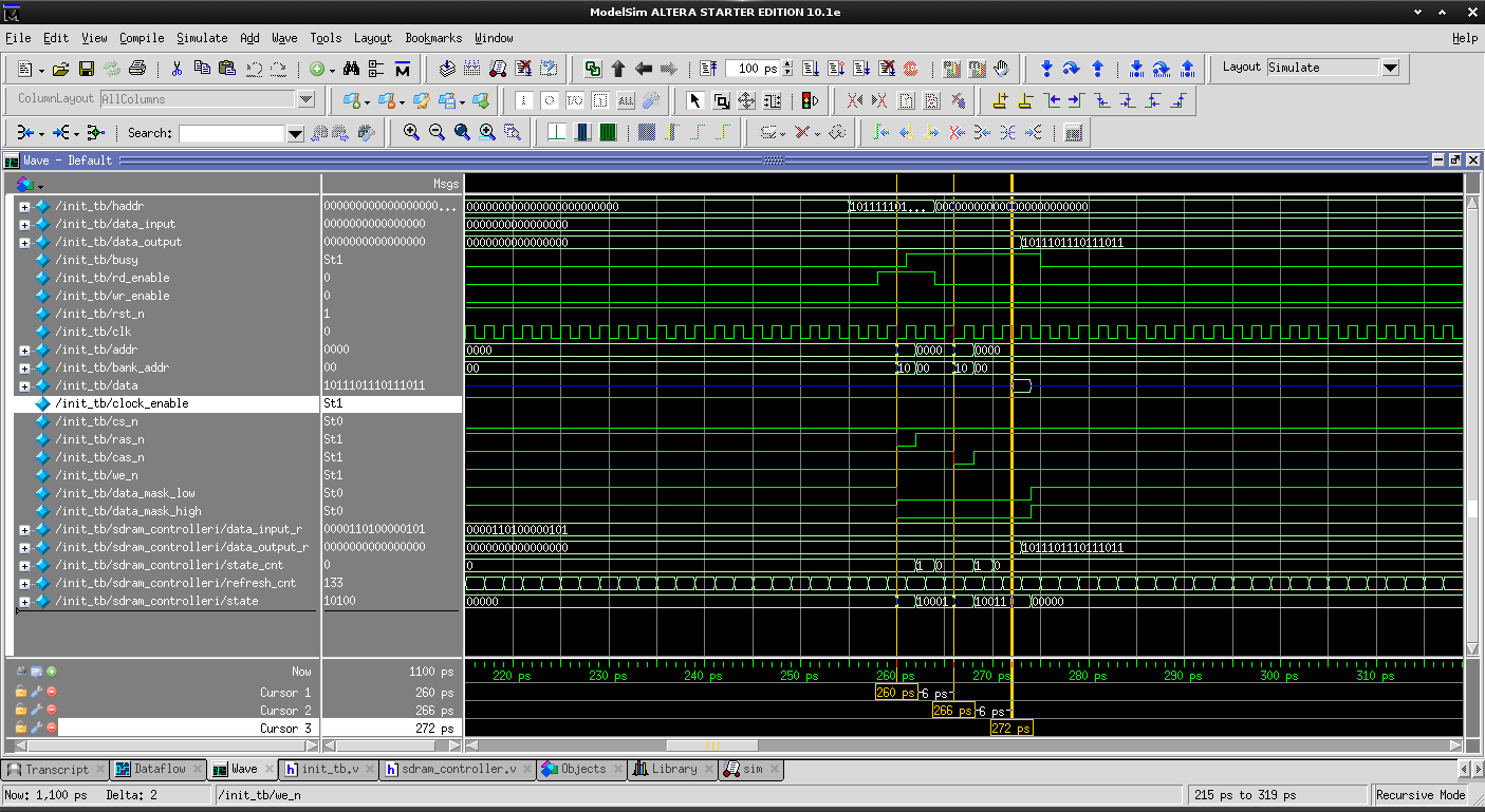
Read operation showing:
- Bank Activation & Row Address Strobe
- Column Address Strobe with Auto Precharge set
- Data on bus
## Test Application
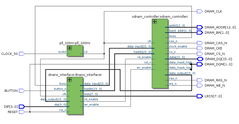
*Figure - test application block diagram*
The test application provides a simple user interface for testing the functionality
of the sdram controller.
Basics:
- The clock input should be 50Mhz (a pll multiplies it up to 100Mhz)
- One push button is used for `reset`
- A Second push button is used for `read` and `write`
- single click for `write`
- double click for `read`
- A 4-bit dip switch is used for inputting addresses and data
- Upon `reset` the read/write addresses are read from the dip switch
- When `writing` the dip switch is data is written to the sdram
- Address and data busses are greather than 4 bits, data is duplicated to fill the bus
- 8 LEDs are used to display the data read from the sdram. The data but is 16-bits, high and low bytes are alternated on the LEDs about every half second.
## Project Status/TODO
- [x] Compiles
- [x] Simulated `Init`
- [x] Simulated `Refresh`
- [x] Simulated `Read`
- [x] Simulated `Write`
- [x] Confirmed in De0 Nano
## Project Setup
This project has been developed with altera quartus II.
## License
BSD
## Further Reading
I didn't look at these when designing my controller. But it might be good to take a look at for ideas.
- http://hamsterworks.co.nz/mediawiki/index.php/Simple_SDRAM_Controller - featured on hackaday
- http://ladybug.xs4all.nl/arlet/fpga/source/sdram.v - Arlet's implementation from a comment on the hackaday article